Midpoint Report
Current Status
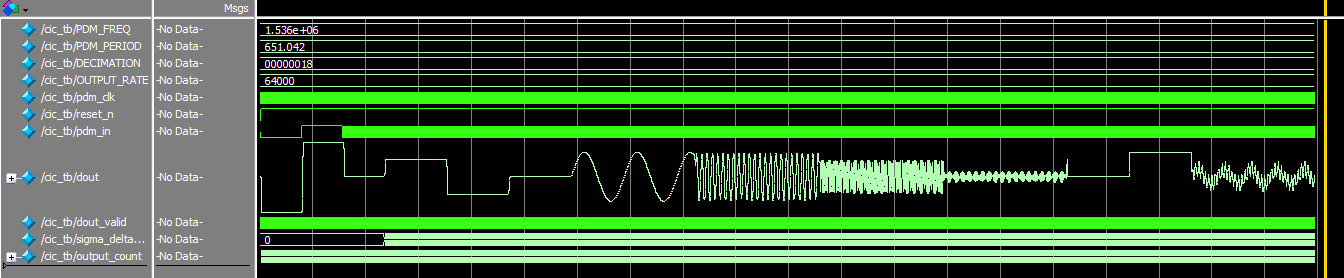
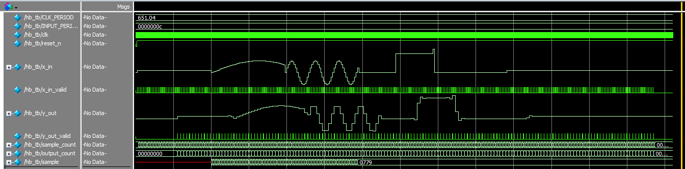
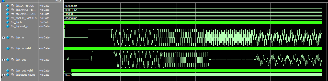
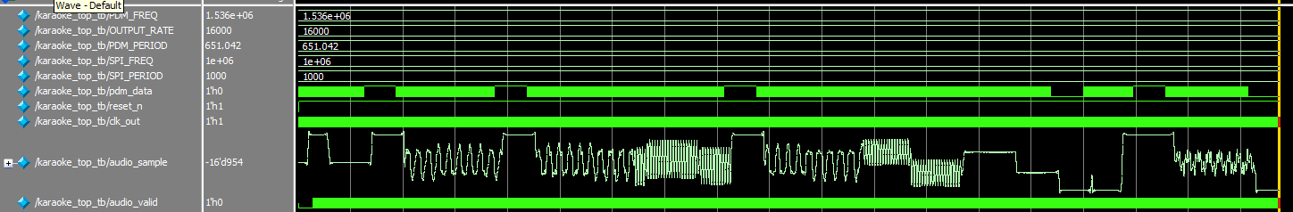
As of this project’s midpoint checkoff (11/20/25), the microphone is somewhat functional and sends audio samples to the FPGA board as desired. The FPGA then performs decimation on the signal by applying one CIC filter, one half-band filter, and one FIR filter, in that order. The CIC filter first decimates the 1.536 MHz PCM input by a factor of 12 through 4 stages to output a 64 kHz 16-bit PCM. The 4 initial integrator blocks accumulate the PDM stream while the decimator takes one out of 12 values. The 4 combs then compute successive differences between delayed samples, which means that they effectively undo the integrator buildup and restore a band-limited approximation of the original signal at the lower sample rate. The half-band filter is a fancy and more efficient FIR filter, using the properties of specific coefficients to halve the number of multiplications and make it more resource-efficient. The coefficients for the half-band were found by specifying a desired passband of 3950 Hz and stopband of 7900 Hz, along with a set decimation ratio of 2 (as half-bands are hardcoded to have) and number of taps, and passed all those parameters into the remez Python function. Essentially, we used this half-band filter to lower the resource strain and still decimate by 2 so we went from a 16-bit 64 kHz PCM to a 32 kHz 16-bit PCM. The FIR filter coefficients were found by calculating the passband ripple and stopband attenuation that results from the first CIC and halfband filters, and specifying the targeted values (around +- 3dB ripple and 60 dB attenuation at least). The FIR filter also had a decimation ratio of 2 to bring down the final frequency to 16 kHz (with a Nyquist of 8 kHz) that maintains all signals required ot distinguish tones during singing. All filters have a one-cycle output pulse that is asserted when there is a new valid value available. This is passed in to the SPI module, along with the final 16-bit and 16 kHz decimated PCM values, to be sent to the MCU.
This process of figuring out the coefficients was extremely difficult due to differences between what we had planned and what was possible. We had originally planned for a 144 decimation ratio starting from a 2.304 MHz PDM rate, with 2 halfbands (x4, x3) in between the CIC (x12) and compensation FIR filter (x1). However, we were not aware that halfbands were only as efficient as they are when they are at x2 decimation. Then, given the limited resources on the FPGA and the slowly mounting number of LUTs as we implemented the filters, we came to the decision that only a single halfband (x2) filter would be possible. Our final plan was the 12x, 4-stage CIC filter, than a single halfband (x2) filter, and the final compensation FIR filter that also decimated by 2. Every single iteration of this pipeline required re-calculating feasible coefficients for the halfbands and FIRs, which took effort and learning of a new section of the matplotlib library in Python. It also took a while implementing a pipeline on the halfband and FIR filters, along with shift-adding to reduce multiplication and, in extension, resource usage.
As the FPGA sends these values to the MCU over SPI, where it proceeds to first apply Z-Score normalization with the intent of maintaining amplitude measurement accuracy; it is also adjusted to account for the CIC filter gain. Note that the MCU is configured in such a way that the SPI transactions automatically send data directly to a buffer in memory via the DMA peripheral, so as to reduce the amount of processing that the core itself needs to do. Next, a Hanning window is used to reduce the signal’s spectral leakage, after which it utilizes the ARM math library functions to actually apply the FFT and take the magnitude of the resulting frequencies. From this, the dominant frequency is found and subsequently output as a note (ex. A3, B4, C5, etc.) in Segger’s Debug terminal. Additionally, while this is all occurring, a data-transfer-complete flag and an FFT-complete flag are constantly being set and reset, so that the program knows when it can start the next round of computations. (See the Flowchart section below for more specific details about the MCU’s general routine and functions.)
From here on out, the team will need to get the LCD and speaker(s) working and properly interfaced with the current system, such that various songs and their lyrics can be played and displayed, respectively. There will also need to be some sort of song-selection mechanism integrated into the process. Moreover, the team has a few timing/latency concerns — regarding the delay between input audio signals and their processed outputs, in particular, as displayed in the verification waveforms below — that will need to be addressed. However, because the riskiest element of the project has already been successfully implemented, completing the rest of these tasks should not be as big of a problem.
Midpoint Specifications
Proficiency
- Clear and concise written summary of current status
- Schematics of all breadboarded circuits
- Block diagram of system components and the interfaces between them
- Hardware demo functioning (potentially with some minor bugs)
- More than 25% of the way to the final deliverable
- Clear description of microcontroller routines
- All external parts ordered
- PDM microphone
- LCD
Excellence
- All interfaces in the block diagram defined (e.g., SPI, I2C, GPIO)
- Hardware demo functioning well
- Writing is well organized
- Solid grammar or spelling issues (no more than a few minor errors which do not detract from the point).
- Completed riskiest element of the project
- FPGA implements all three filters to perform decimation appropriately
- Microphone interfaces with the FPGA and MCU
- More than 50% of the way to the final deliverable
Technical Documentation
The source code for this project can be found in the associated GitHub repository.
Block Diagram
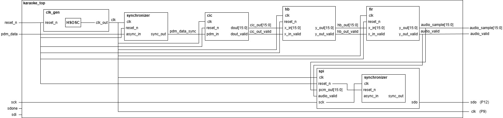
The block diagram in Figure 1 depicts the general architecture implied by the SystemVerilog code.
Schematic
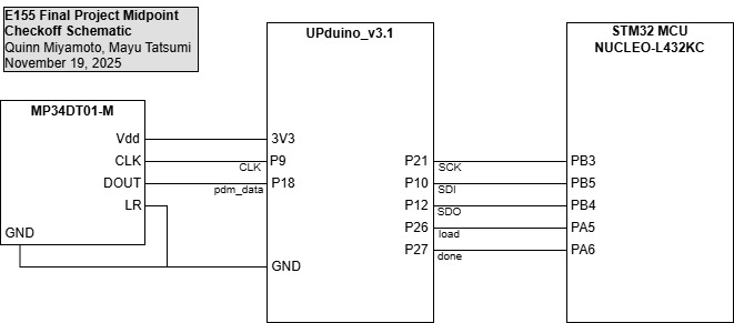
Figure 2 above depicts all of the components comprising the breadboarded circuit at the time of the midpoint checkoff. This includes the PDM microphone, FPGA, and MCU; note that while the connections between the FPGA and MCU did not need to be explicitly outlined, as they are both on-board elements of the PCB that are hooked up internally, these were shown for the sake of clarity, especially regarding the SPI transactions. Overall, the microphone and FPGA interfacing was done in accordance with the MP34DT01-M datasheet. The most prominent feature of note is the tying of the LR port to ground, as that configures a DOUT signal pattern of valid data when the CLK signal is low and high impedance when CLK is high.
Flowchart
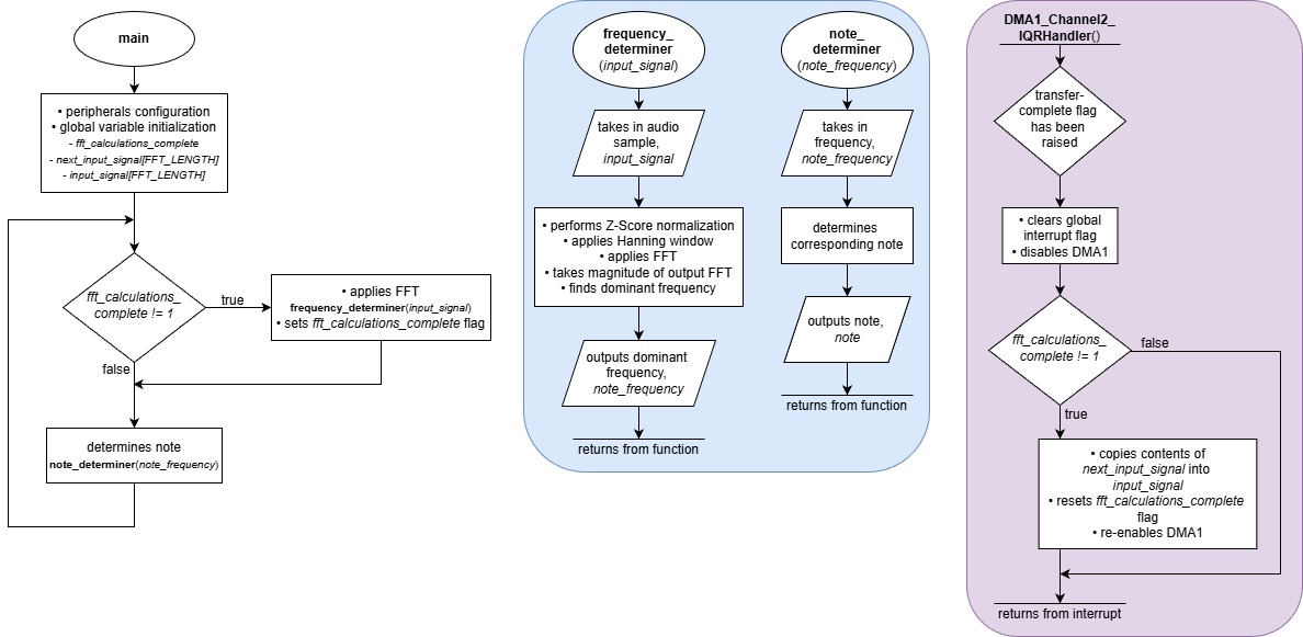
The Figure 3 flowchart provides a detailed overview of the microcontroller’s most significant routines.
First and foremost, the main loop’s primary jobs are to 1) configure the MCU and all of its relevant peripherals, 2) continuously apply an FFT to the detected audio samples — which are, again, transmitted to the controller via SPI — in order to determine the dominant frequencies, and 3) output the corresponding note. This notably requires the help of two custom functions, frequency_determiner and note_determiner. The former makes use of the ARM math library to actually perform the FFT calculations (with some pre-processing work done to ensure greater accuracy and resolution), after which an fft_calculations_complete flag is set. Meanwhile, the latter comprises what is essentially a look-up table to output the dominant frequency as a note that is in human-readable terms. Finally, the DMA1_Channel2_IRQHandler deals with any interrupts that trigger as a result of the SPI-to-DMA-transfer-complete flag being set. More specifically, it waits until the fft_calculations_complete flag is high to copy the contents of the SPI data register (i.e. whatever audio sample the FPGA is sending over at the time) to a second buffer, named input_signal, for frequency_determiner to subsequently process; then, it resets the fft_calculations_complete so that the process may begin anew.
Verification
Various means of verification were used to ensure the project’s accuracy, including the following simulation waveforms, as well as actual experimentation with the hardware itself.
Testbench Simulation